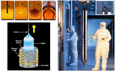
Imagine an alumina ceramic electric furnace filled with ultra high purity chunks of silicon, heat under a gas blanket of argon to keep the 3000F melt from reacting with air oxygen or moisture. Ironically air contains argon, this is how gas companies pressure swing concentrate argon, then compress cool & bottle it for use in TIG welding or similar as a shielding gas for the same reason, it prevents air from reacting with the super hot metals created by the electric arc formed during TIG (Tungsten Inert Gas) welding.
Known as the Czochralski Method of growing large single crystal boules, later cut into wafers, then subjected to hundreds of processing stages at Chip Fabs to make computer chips like CPU, GPU, SOC, as common examples of cutting end integrated circuits or the brains of computers, tablets, smartphones, laptops, desktops, servers, even all the integrate chips in modern automobiles which each contain more than 100 chips, the same reason that the global chip shortage during COVID19 supply chain disruption caused many automakers to stop production of cars, trucks, SUV, buses and other modern vehicles with ADAS, computers like the ECU or engine control unit, VSC vehicle stability control, ESC electronic stability control, LKA or lane keep assist, RSA or road sign assist, Pre-Collision Avoidance, Adaptive Radar Enhanced Cruise Control, AHB automatic high beams or any of the other such systems, all of which make use of digital computers linked over OBDII networks in the car & its famous dash connections that allows a diagnostic tool to be plugged into to a newer vehicle to determine what is wrong if the MIL or master warning light illuminated on the dashboard indicated a problem. On the OBD tool you get codes you can look up online to find what they mean. Genius Gordon Teal pioneered optimizing the large single crystal production & designed many early advanced versions of such furnaces.
These giant boules of silicon single crystal have weigh up to 600 kilograms yet can be held by a single 1mm thread of silicon at the top since silicon has incredible tensile strength but also super brittle worse than most kinds of glass, so the thread of silicon holding the heavy boule can be broken by tapping it with a metal tool, the same way you could easily shatter a glass screen cover over the smartphone screen by hitting it with a metal tool hard enough. You can ad a protect glass screen cover over the other glass to act like a sacrificial protective layer so that it cracks instead of the screen glass if you drop you phone on a sharp rock or metal or something hard enough the crack the screen. See the following collection of images as a Dynamic Island image via the following link (https://waferpro.com/wp-content/uploads/2017/05/growing-silicon-ingot.jpeg.webp)
From Wikipedia
Czochralski method, also Czochralski technique or Czochralski process, is a method of crystal growth used to obtain single crystals(monocrystals) of semiconductors (e.g. silicon, germanium and gallium arsenide), metals (e.g. palladium, platinum, silver, gold), salts and synthetic gemstones. The method is named after Polish scientist Jan Czochralski, who invented the method in 1915 while investigating the crystallization rates of metals. He made this discovery by accident: instead of dipping his pen into his inkwell, he dipped it in molten tin, and drew a tin filament, which later proved to be a single crystal. The process remains economically important, as roughly 90% of all modern-day semiconductor devices use material derived from this method.
The most important application may be the growth of large cylindrical ingots, or boules, of single crystal silicon used in the electronics industry to make semiconductor devices like integrated circuits. Other semiconductors, such as gallium arsenide, can also be grown by this method, although lower defect densities in this case can be obtained using variants of the Bridgman–Stockbarger method. Other semiconductors such as Silicon Carbide are grown using other methods such as physical vapor transport.

Transforming giant crystals into trillions of transistors mirrors how precision engineering in industrial valves has evolved—scaling from simple mechanical parts to high-performance, automated flow control systems. Just as crystal miniaturization drives computing, valve innovation fuels efficiency and safety across modern process industries.
ReplyDeletePTFE Lined Valve Manufacturer in India